MacDermid Alpha Center of Excellence in Advanced Electronics Manufacturing & Skills Development
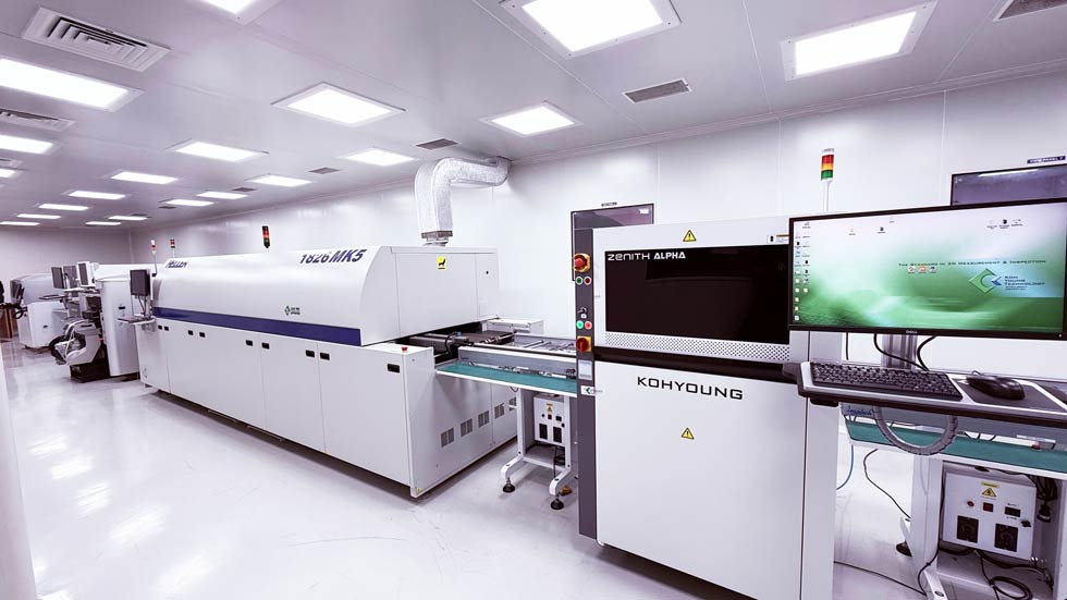
The Surface Mount Technology (SMT) Fabrication Facility at the Central Electronics Centre is housed at the MacDermid Alpha Center of Excellence in Advanced Electronics Manufacturing & Skills Development. The facility offers a fully integrated environment for precision assembly of electronic circuit boards. The facility encompasses all critical stages of SMT manufacturing—solder paste printing, solder paste inspection (SPI), high-speed pick-and-place assembly, reflow soldering, and automatic optical inspection (AOI).
Designed to support both prototyping and low-to-medium volume production, the SMT line is equipped with advanced automation and inspection systems to ensure repeatability, reliability, and process control. It serves as a valuable resource for researchers, product developers, and industry partners engaged in electronics design, fabrication, and quality assurance.
Solder Paste Printing
Solder paste printing marks the first and one of the most critical stages in the surface-mount technology (SMT) assembly process. At CEC, this process is performed using a high-precision, fully automated solder paste printing machine that ensures accurate deposition of solder paste on PCBs through stainless steel stencils and dual squeegee blades.
Precision stencil printing with automated alignment ensures consistent solder deposition—laying the groundwork for reliable surface-mount assembly.
Our system employs an advanced control mechanism to maintain consistent print quality and alignment. Fiducial point alignment between the stencil and PCB—ensuring a minimum of 3 mm clearance from the board edge—is critical to achieving precise pattern registration. The use of a 29″x29″ stainless steel stencil provides superior edge definition and repeatability, even over extended use.
The printing head consists of two 45° squeegee blades that apply uniform pressure to deliver consistent paste volume across all pads. With a conveyor width of 450 mm, the machine can accommodate a broad range of PCB sizes. We use only lead-free solder paste in accordance with environmental and regulatory standards, supporting both research and industry-compliant manufacturing.
This process sets the foundation for downstream assembly quality, and is tightly controlled to meet the stringent requirements of high-reliability electronic products.
Precision Deposition Using Stainless Steel Stencils
Optimized Dual-Blade Squeegee System
Automated Alignment with Fiducial Accuracy
450 mm Conveyor with Lead-Free Process
Solder Paste Inspection
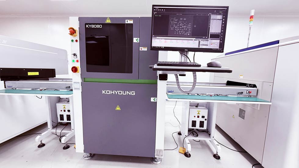
Solder Paste Inspection is a critical quality control step in the Surface Mount Technology (SMT) assembly process, ensuring the reliability and precision of printed circuit board (PCB) production. At CEC, the SPI system is employed immediately after solder paste deposition to evaluate key parameters such as the height, volume, and shape of the paste deposits across the entire PCB surface.
Accurate solder paste deposition is the foundation of reliable SMT assembly—our 3D SPI system ensures every print meets precision standards before components are placed.
Using advanced 3D measurement techniques, the SPI machine utilizes a combination of 360° RGB ring lighting and cross-angle twin projectors to perform high-fidelity inspection. This allows for clear delineation of paste boundaries and accurate detection of deposition defects, including bridging, insufficient volume, and misalignment. The system operates with a maximum measurable paste height of 400 µm and is capable of resolving minimum deposits as small as 150 µm (rectangular) and 200 µm (circular).
The process requires the Gerber and CAD data for precise stencil and pad alignment. Additionally, the SPI system supports automatic computation of stencil offsets and alignment verification, ensuring that any anomalies are flagged early in the production line.
3D Optical Inspection
High Sensitivity
Early Defect Detection
CAD & Gerber Integration
Pick & Place Assembly
The Pick & Place stage is central to the automated assembly of surface-mount electronic circuits. This high-speed system is designed to accurately position a variety of components—including resistors, capacitors, and integrated circuits—onto printed circuit boards (PCBs) with exceptional precision.
Fast, flexible, and accurate—our Pick & Place system forms the core of high-throughput, precision electronics assembly.
The equipment is configured with 36 front and 36 rear feeder stations, supporting a wide range of component sizes and packaging formats via reels or trays. Component pickup is performed using pneumatic suction nozzles, with 24 nozzle sizes available to match varying device geometries and ensure secure handling.
To accommodate diverse assembly requirements, the machine supports multiple feeder widths, including 8 mm, 12 mm, 16 mm, 24 mm, and 32 mm. With a maximum placement speed of 42,000 components per hour (CPH), the system is engineered for both high throughput and placement accuracy—critical in modern electronics manufacturing.
This process not only ensures rapid and consistent assembly but also aligns with industry standards for quality and scalability in prototype and volume production environments.
High-Speed Precision
Flexible Component Handling
Adaptable Nozzle System
Versatile Feeder Options
Reflow Oven
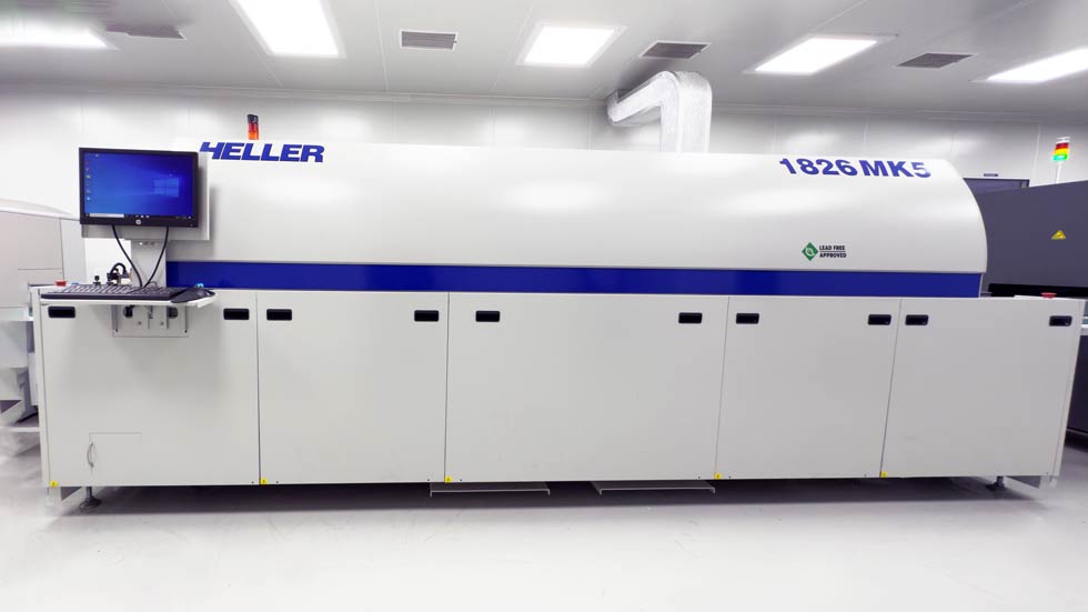
The reflow oven is a critical stage in the surface-mount assembly process, where soldering of surface-mounted electronic components to the PCB takes place. At CEC, the reflow soldering process is carried out using a tunnel-type reflow oven equipped with a precision-controlled conveyor system. This conveyor transports assembled boards through a series of temperature-regulated zones, facilitating a consistent and uniform soldering profile across all components.
Through carefully profiled thermal zones, the reflow oven transforms solder paste into robust, high-integrity electrical connections.
Operating at peak temperatures of up to 350°C, the oven is divided into multiple heating zones—each carefully calibrated to manage the thermal ramp-up, soak, reflow, and cooling phases. This staged approach ensures that the solder paste melts and reflows precisely at the joints between component leads and PCB pads, achieving strong metallurgical bonds without component stress or misalignment.
The final phase of the process involves controlled cooling, which solidifies the solder and locks components in place, preserving both the mechanical and electrical reliability of the assembly. CEC’s reflow process is tuned for repeatability and precision, aligning with best practices for high-quality electronics manufacturing.
Multi-Zone Heating Profile
High-Temperature Precision
Automated Conveyor Integration
Reliable Joint Solidification
Automatic Optical Inspection
Automatic Optical Inspection (AOI) is an essential quality control step in the surface-mount assembly process, implemented to identify assembly defects with high precision and consistency. At the Central Electronics Centre (CEC), AOI is deployed immediately after the reflow process to verify the integrity of each assembled PCB before it advances to functional testing or packaging. This early detection mechanism is crucial for maintaining yield quality and ensuring long-term reliability of the final product.
AOI enhances quality assurance by detecting minute assembly errors with micron-level accuracy, ensuring only defect-free PCBs proceed to the next stage.
At CEC, our AOI system utilizes a high-resolution 8-megapixel 3D vision camera to meticulously scan each assembled PCB for deviations in geometry, alignment, and solder joint integrity. It measures component height, width, and placement accuracy, using reference data extracted from CAD XY coordinates and Gerber files to compare each board against its design intent. The system conducts a comprehensive analysis of each component and solder joint, flagging defects such as misalignment, pad overhang, incorrect polarity, coplanarity issues, solder bridging, insufficient or excessive solder, and tombstoning.
This non-contact, high-speed inspection process significantly enhances inspection accuracy and repeatability, while simultaneously reducing production rework, cost, and cycle time. AOI serves as a key contributor to process reliability, enabling CEC to uphold stringent quality standards in complex and high-density PCB assemblies.
High-Precision 3D Imaging
Comprehensive Defect Detection
Data-Driven Verification
Enhanced Inspection Efficiency
Part removal and replacement
Mass production: 20~25 working days
The fastest delivery time is 3 days


